Fundamentals
First-principle Calculations
With the silicon metal-oxide-semiconductor field-effect transistors rapidly reaching its physical limits, continual miniaturization of the channel length to improve the device performance is not sustainable. Novel device structures and electronic materials are required to further meet the needs of digital circuits after the current MOSFET technology reaches its physical limits. One of the contributions of the theoretical calculations is to propose new requirements of materials and new constructions.
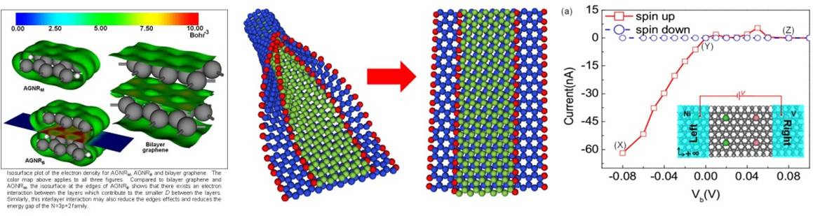
Due to their unique advantages, low dimensional systems, such as graphene and its derivatives, have attracted considerable attention experimentally as well as theoretically due to their potential applications in electronic and spintronic devices. Over the past decades, a detailed knowledge of the electric and magnetic properties in these low dimensional systems has been obtained. By using recently popular first-principles density functional theory (DFT), such as Vienna ab initio simulation package (VSPA), CASTEP, DMOL3 and quantum transport calculations based on NEGF formalism with the help of the Atomistix Toolkit, we study the electronic and transport properties of graphene derivatives, bilayer graphene ribbion and hybrid configuration with Boron nitride embedded graphene ribbon. Our present works show the rich electronic and magnetic behaviors in these systems. We also established the mechanism to clarify the physics behind. Due to possible existence of half-metallicity (HM), perfect spin filter and even negative differential resistance (NDR), we expect that prediction of more new features of low-dimensional systems will inspirit scientists to study how to synthesize the materials alike. It is our hope that our findings can impulse further works in both theory and experiment.
Related Publications:
1. K. T. Lam and G. Liang, ˇ°An Ab Initio Study on Energy Gap of Bilayer Graphene Nanoribbons with Armchair Edgesˇ±, Appl. Phys. Lett. 92, 223106 (2008).
2. K. T. Lam, Y. Lu, Y. P. Feng and G. Liang, "Stability and electronic structure of two dimensional Cx(BN)y compound", Appl. Phys. Lett. 98, 022101 (2011).
3. You Qian, Kai-Tak Lam, Chengkuo Lee and Gengchiau Liang, The effects of interlayer mismatch on electronic properties of bilayer armchair graphene nanoribbonsˇ±, (Submitted to Carbon).
4. Haixia Da, Yuan Ping Feng and Gengchaiu Liang, ˇ°Transition-Metal-Atom-Embedded Graphane and its Spintronic Device Applicationsˇ±, (Under revision in Jour. Phys. Chem. C)
Thermoelectric properties of low-dimentional materials
The important characteristic for thermoelectric material is the dimensionless thermoelectric figure of merit, ZT =S^2¦ŇT/k, where S, ¦Ň, T and k are the Seebeck coefficient, electrical conductivity, absolute temperature and thermal conductivity, respectively, while S^2¦Ň alone is commonly known as power factor whichonly focuses on the material performance of electrons when thermal conductivity at the two end reservoirs can be ruled out. The difficulty of maximizing ZT and power factorlies in the fact that the above parameters are generally interdependent. Therefore, it is a challenge to develop advanced thermoelectric materials with an optimization of these conflicting properties to increase ZT and power factor. Two approaches of thermoelectric materials were brought forward. One is using new categories of advanced bulk thermoelectric materials, such as ˇ®phonon-glass electron-crystalˇŻ (PGEC) materials, which can conduct heat like a glass while conduct electricity like a crystal. The alternative is using low-dimensional materials systems, such as quantum wells, quantum wires and quantum dots because quantum confinement effects are able to enhance power factor and reduce thermal conductivity. Among these, one-dimensional semiconducting nanowires and graphene nanoribbons have attracted considerable interests.
Related Publications:
1. G. C.Liang, W. Huang, S. K. Chee, J.-S. Wang, and J. H. Lan, "Geometry effects on thermoelectric properties of silicon nanowires based on electronic band structures," J. Appl. Phys. 107, 014317 (2010).
2. W. Huang, S. K. Chee, and G. C. Liang, "Theoretical study on thermoelectric properties of Ge nanowires based on electronic band structures," IEEE Electron Device Lett. 31, 1026-1028 (2010).
3. W. Huang, J.-S. Wang, G. C. Liang, "Theoretical study on thermoelectric properties of kinked Graphene Nanoribbons," Phys. Rev. B 84, 045410 (2011).
|
Transport Properties
Ballistic transport approach
The Landauer formalism in the linear response regime based on nonequilibrium GreenˇŻs function (NEGF) formalism has been widely used to investigate the thermoelectric properties of the different materials due to its powerful ability to compute the transmission coefficient of electrons and phonons in the atomic systems. However, it is very computationally expensive for calculation of the transmission coefficient of the periodic supperlattic system with many numbers of atoms or with multiple orbital basis set in the unit cell . On the other hand,a ballistic transport approach is introduced to study electron and phonon transport properties. The transmission can be represented with group velocity and density of states, which can be directly obtained from the band structures for electron and phonon. This approach is more time-efficient for superlattice systems without consideration of scatterings.
Quantum transport in nanoscale systems and devices
Recent advances in electronics technology have ushered in devices utilizing components with length scales in the nanometers. The Intel Core i7 processor, for example, is manufactured using a 32 nm process. According to MooreˇŻs law, the number of transistors fitted in a chip doubles every two years. And so as more transistors are fitted into a chip, the sizes of the components become even smaller. Projecting the advance of processor technology for the next few years, we would thus see electronic components approaching the sizes of atoms, i.e., around 0.1 nm. For such small sizes, quantum mechanical effects become significant. For instance, effects such as quantum interference and quantum tunneling, which may have been ignored previously, become the dominating factors because we now have to deal directly with the current-carrying quantum particles, e.g., electrons and holes, and how they behave in the device.
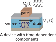 A full quantum-mechanical treatment is necessary to theoretically understand how current-carrying particles behave in nano-devices. In our group we primarily employ nonequilibrium GreenˇŻs functions (NEGF) techniques to derive analytical expressions for physical properties such as the current through the device and the conductance of the device. These analytical expressions are then numerically calculated for specific device configurations. The figure at the left is an illustration of a device consisting of a current source, a drain, and a top gate. When a source-drain potential, VDS, is attached current-carrying particles would flow from the source to the drain. The gate potential, VG, modulates the amount of current flowing from the source to the drain. The current through the device can be calculated using NEGF. In general, the source-drain potential and the gate potential can vary in time, as shown in the figure. The top gate, for example, can vary in the form of a square or a sine wave. As another example, the source-drain potential may be from an alternating-current generator or a battery that is suddenly switched on. Because the applied potentials are varying in time, the resulting current ends up also varying in time. We employ time-dependent nonequilibrium GreenˇŻs functions (TD-NEGF) techniques to determine this time-dependent current. A full quantum-mechanical treatment is necessary to theoretically understand how current-carrying particles behave in nano-devices. In our group we primarily employ nonequilibrium GreenˇŻs functions (NEGF) techniques to derive analytical expressions for physical properties such as the current through the device and the conductance of the device. These analytical expressions are then numerically calculated for specific device configurations. The figure at the left is an illustration of a device consisting of a current source, a drain, and a top gate. When a source-drain potential, VDS, is attached current-carrying particles would flow from the source to the drain. The gate potential, VG, modulates the amount of current flowing from the source to the drain. The current through the device can be calculated using NEGF. In general, the source-drain potential and the gate potential can vary in time, as shown in the figure. The top gate, for example, can vary in the form of a square or a sine wave. As another example, the source-drain potential may be from an alternating-current generator or a battery that is suddenly switched on. Because the applied potentials are varying in time, the resulting current ends up also varying in time. We employ time-dependent nonequilibrium GreenˇŻs functions (TD-NEGF) techniques to determine this time-dependent current.
As a short outline on how the current is determined, we construct contour-time GreenˇŻs functions employing a Keldysh contour that starts at time t = 0, proceeds to time t, and then goes back to time t = 0. Analytical expression for these contour-ordered GreenˇŻs functions can then be derived from their corresponding Dyson equation (and using Feynman diagrammatic techniques) and quantum equations of motion. LangrethˇŻs theorem and analytic continuation are then used to restore the GreenˇŻs functions back to using real-time parameters. Physical variables such as the current and conductance are then calculated using the derived real-time GreenˇŻs functions. Computationally, the procedure is complicated because there are several multiple integrals that must be calculated numerically.
A special case is when the potentials are not varying in time. For such a case, the system is still not in equilibrium and the transport is considered at a steady state. There are several analytical approaches in dealing with steady-state quantum transport. The TD-NEGF approach described above is also applicable to the problem except that the limit for the time t ->  should be taken. Taking such a limit would actually result in significant simplifications to the calculation and, for specific cases, reproduce the well-known Landauer formula. should be taken. Taking such a limit would actually result in significant simplifications to the calculation and, for specific cases, reproduce the well-known Landauer formula.
Related Publications:
|
Device Applications
Electronic Devices
Nano-FETs
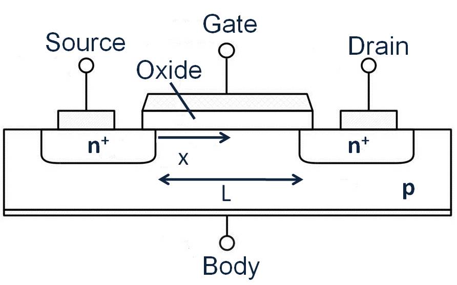
Above figure shows a typical n-type MOSFET structure in cross-section. As the Gate bias increases, a depletion layer (of electrons) formed at the Oxide-Body interface, forming a channel for electron transport from the Source to the Drain. The device performance can be increased by reducing the channel length, L.
In the past few decades, the performance improvement of silicon metal-oxide-semiconductor field-effect transistors (MOSFETs) had been driven mainly by channel length scaling. However, it is impossible to reduce the channel length indefinitely due to physical limitations. From classical transport models, the current of a MOSFET can be divided into two regions. For VGS > VTH,
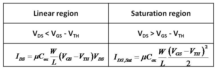
From the above equations, it can be easily seen that by reducing the channel length, the drive current can be increased accordingly. However, aggressive reduction in channel length leads to other undesirable effects such as:
- Drain-induced barrier lowering (DIBL) which affects the output conductance and threshold voltage. As the channel length reduces, the electric field in the transport direction becomes stronger, and the gate control weakens. While increasing the oxide capacitance by using high-k dielectric material can counteract DIBL, further reduction in channel length would increase the effect of DIBL and eventually the device fails as it cannot be controlled by the gate bias.
- Velocity saturation whereby the current no longer increases as the channel length decreases. This is due to the increasing carrier scattering in high electric field due to the short channel length and the carrier group velocity no longer increases as channel length decreases.
As such, continual improvement in digital MOSFET devices cannot rely on channel length reduction alone. New materials with higher carrier mobility (¦Ě) such as III-V compound semiconductors (GaAs, GaN, InAs), carbon-based material (graphene, graphane, carbon nanotube, graphene nanoribbon) and nanostructure materials (thin-film, nanowire, nanotubes), as well as novel MOSFET structure such as double- and multi-gated MOSFET can be used to enhance the performance of MOSFET.
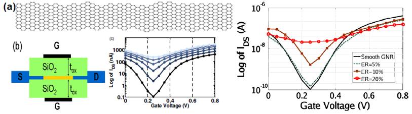
Our group has investigated the device performance of double-gated graphene nanoribbon MOSFETs focusing on the effect of ribbon width, ribbon edge roughness and contact materials. The figure below on the left shows: (a) The atomic structure of a rough-edge GNR. (b) Schematic of the double-gated GNR MOSFET. (c) The transfer characteristics of the smooth-edge GNR MOSFET with respect to different widths where the current increases as the width increases due to the reduction in the energy bandgap. The figure below on the right shows the effect of edge roughness on a GNR MOSFET with ribbon width of 1.2 nm.
Related Publications:
1. Zuan-Yi Leong, Kaitak Lam, and Gengchiau Liang, "Device Performance of Graphene Nanoribbon Field Effect Transistors with Edge Roughness Effects: A Computational Study," 13th International Workshop on Computational Electronics (IWCE 2009),Bejing, China, May 27-29, 2009.
2. Gengchiau Liang, "Width Effects in Ballistic Graphene Nanoribbon FETs," IEEE International Nanoelectronics Conference 2008, Shanghai, China, Mar. 24-27, 2008.
3. G. C. Liang, N. Neophytos, M. Lundstrom, and D. Nikonov, "Contact Effects in Graphene Nanoribbon Transistors," Nano Lett. 8(7), 1819-1824 (2008).
RF transistor
With the wide-spread usage of mobile communication devices, the study of the performance and power consumption of radio frequency (RF) electronics is becoming more important. TodayˇŻs 3G mobile phone communicates wirelessly using frequencies in the 2 GHz range. The technology has the capability of moving a lot of information through a bandwidth of about 3 Mbps and the demand for higher data transfer rate is increasing. As such, we expect the research into future devices and circuits with the ability to handle signal frequencies in ranges that are much higher than todayˇŻs standards at a lower energy cost to be of great importance.
The essential components in RF electronics are mixer and amplifier, and the speed of the transistors which make up these devices strongly affects the operating frequency of the devices. Recent study on graphene mixer indicates a RF performance of 10 GHz and optimization can further enhances the operating frequency. However, graphene FET also exhibit a high output conductance due to the zero-bandgap, leading to a lower gain and is not suitable for amplifier applications. (Figure from Science)
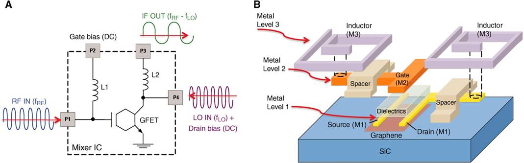
Our research focus on the RF performance of semiconducting graphene nanoribbons (GNR), with the possibility of providing high cut-off frequency, low noise figure, high gain, high output power, high maximum frequency of oscillation, optimum ION and IOFF and a low gate resistance. Our study involves analysis of different widths of the GNR for RF applications, as well as the effect of phonon-electron interaction on the RF performances of GNR devices.
Related Publications:
Energy Efficient Devices
Thermoelectric devices
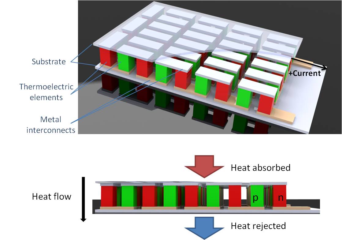
The demand for alternate source energy has been increasing over the years since the crisis of running out of fossil fuel reserves is becoming imminent. To solve this crucial challenge, thermoelectric materials have received growing attention in the recent years as they can generate electricity from heat which is normally lost to the environment. The thermoelectric power generation, cooling and heating applications are based on solid-state devices with no moving parts, which leave the material characteristics as the measures of efficiency. The thermoelectric properties are dependent on the packing conditions, temperature at two reserviors and channel geometry structures.
Related Publications:
1. G. C.Liang, W. Huang, S. K. Chee, J.-S. Wang, and J. H. Lan, "Geometry effects on thermoelectric properties of silicon nanowires based on electronic band structures," J. Appl. Phys. 107, 014317 (2010).
2. W. Huang, S. K. Chee, and G. C. Liang, "Theoretical study on thermoelectric properties of Ge nanowires based on electronic band structures," IEEE Electron Device Lett. 31, 1026-1028 (2010).
3. W. Huang, J.-S. Wang, G. C. Liang, "Theoretical study on thermoelectric properties of kinked Graphene Nanoribbons," Phys. Rev. B 84, 045410 (2011).
Optoelectronic devices
Related Publications:
New Functional Devices
RTDs
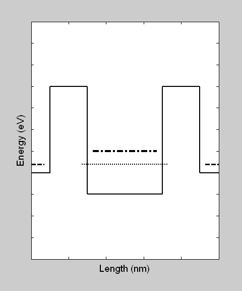
The edge roughness effects of graphene nanoribbons on their application in resonant tunnelling diodes with different geometrical shapes (S, H, and W) were investigated. 60 samples for each 5%, 10% and 15% edge roughness conditions of these differently shaped graphene nanoribbon resonant tunnelling diodes had been randomly generated and studied. Firstly, it was observed that edge roughness at the barrier regions decreases the effective barrier height and thickness, which increases the broadening of the quantized states in the quantum well due to the enhanced penetration of the wave-function tail from the electrodes. Secondly, edge roughness increases the effective width of the quantum well and causes the lowering of the quantized states. Furthermore, the shape effects on carrier transport are modified by edge roughness due to different interfacial scattering. Finally, with the effects mentioned above, edge roughness has a considerable impact on the device performance in terms of varying the peak-current positions and degrading the peak-to-valley current ratio.
Related Publications:
1. H. Teong, K. T. Lam and G. Liang, ˇ°A Computational Study on the Device Performance of Graphene Nanoribbon Resonant Tunneling Diodes (GNR RTDs)ˇ±, Jpn. J. Appl. Phys. 48, 04C156 (2009).
2. G. Liang, S. B. Khalid and K.-T. Lam, ˇ°Influence of edge roughness on graphene nanoribbon resonant tunneling diodes,ˇ± J. Phys. D: Appl. Phys. 43, 215101 (2010).
Tunning FETs
The device physics and performance of heterojunction (HJ) graphene nanoribbon (GNR) tunneling field-effect transistors (TFET) with different designs are investigated in this work.? Due to the width-dependent energy bandgap (EG), a single GNR with spatially dependent width naturally yields a heterojunction (HJ) structure to improve the device performance of GNR TFET. By adding small-EG region in the channel near the source and large-EG region in the middle of the channel, the ON- and OFF-state currents (ION and IOFF, respectively) can be tuned. Lastly, we studied the effect of channel length scaling on HJ GNR TFET, and it was observed that a ION/IOFF ratio of 4 order can achieved with a channel length of 10 nm and a drain bias of 0.6 V.
Graphene has opened a new era in electronics and condensed matter since its successful preparation in 2004. The patterned graphene ribbon arise the band gaps due to size confinement and edge effects and their band gaps are width-dependent which obeys three different families. These peculiar properties make graphene ribbon attractive candidates in tunneling field effect transistors (TFET) devices, which have been demonstrated to show better performance with a high subthreshold slope (SS) compared to those based on conventionally semiconductors such as silicon. The transport characteristics and performance evaluation are investigated in heterojunction graphene ribbon.
Related Publications:
1. K.-T. Lam, S.-K. Chin, D. W. Seah, S. Bala Kumar and G. Liang, ˇ°Effect of Ribbon Width and Doping Concentration on Device Performance of Graphene Nanoribbon Tunneling Field-Effect Transistorsˇ±, Jpn. J. Appl. Phys. 49, 04DJ10 (2010).
2. S.-K. Chin, D. Seah, K.-T. Lam, G. S. Samudra and G. Liang, ˇ°Device Physics and Characteristics of Graphene Nanoribbon Tunneling FETsˇ±, T-ED 57, 3144 (2010).
3. K.-T. Lam, D. Seah, S.-K. Chin, S. Bala Kumar, G. Samudra, Y.-C. Yeo and G. Liang, ˇ°A Simulation Study of Graphene-Nanoribbon Tunneling FET With Heterojunction Channelˇ±, EDL 31, 555 (2010).
4. H. Da, K.-T. Lam, S. K. Chin, G. S. Samudra, Y.-C. Yeo, and G. Liang, "Performance evaluation of graphene nanoribbon heterojunction tunneling field effect transistors with various source/drain doping concentration and heterojunction structure," 2010 International Conference on Solid State Devices and Materials, Tokyo, Japan, Sep. 22-24, 2010.
NEM switches
In the recent years, nanoelectromechanical systems (NEMS) have been intensely pursued as a promising solution for future low power switches in nonvolatile memory applications due to its attractive characteristics like abrupt switching and extremenly low OFF-state leakage currents. However, current generation of silicon NEMS based switches requires high activation voltage and low ON-state currents. As a result, utilizing materials with high carrier mobility to obtain a larger drive current which can be actuated at lower voltages has been a major focus in NEMS research.
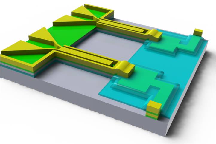
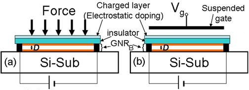
On the other hand, due to their excellent mechanical and electrical properties such as high tensile strength and high carrier mobility, carbon-based material such as carbon nanotube has been actively researched as a potential material for many NEMS devices. Our group investigated a bilayer graphene nanoribbon NEMS device via first-principle simulations. The output characteristics as a function of interlayer distance are calculated, with the proposed device acting as a displacement and a force sensor. The operating mechanism of a bi-stable switch based on this device structure is also explored and in the present floating gate design, a switching gate bias of 5.6 V is required, resulting in an ON-OFF current ratio of 3 orders at a device bias of 20 mV. This minuscule bi-stable device could potentially be implemented in future semiconductor memory devices and radio frequency communication circuitry.
Related Publications:
1. K. T. Lam, C. Lee and G. Liang, ˇ°Bilayer Graphene Nanoribbon Nanoelectromechanical System Device: A Computational Studyˇ±, Appl. Phys. Lett. 95, 143107 (2009).
2.Kai-Tak Lam, Marie Stephen Leo, Chengkuo Lee and Gengchiau Liang, "Design evaluation of graphene nanoribbon nanoelectromechanical devices," Journal of Applied Physics, vol. 110, no. 2, 024302 (6 pages), July 2011.
?
Pseudospin devices
Related Publications:
Thermal spin devices
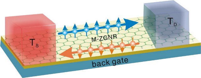
Spin caloritronics, a new exciting research filed, explores the combination of spintronics and thermoelectronics. Graphene has been regarded as a strong candidature for spintronics. Moreover, graphene show some interesting features for thermoelectronics applications. Motivated by these properties, a magnetized ZGNR with temperature bias are used to investigate the physics mechanisms and potential graphene-based spin caloritronics applications using first-principle calculations. We find the unique spin Seebeck effect in the magnetized ZGNR. Moreover, the thermal-induced currents in the magnetized ZGNR can be controlled by controlled by thermal (i.e., temperature), electrical (gate voltage) or magnetic means, thereby providing a rich set of thermal spin components (spin filter, spin diode, spin FET, MR device). Our results show an approach to create and control thermally induced spin-polarized currents in nanodevices and pave the way for carbon-based spin caloritronics.
Related Publications:
1. Minggang Zeng, Yuan Ping Feng, and Gengchiau Liang, ˇ°Graphene-based Spin Caloritronics,ˇ± Nano Lett.11 (3),1369¨C1373,(2011);
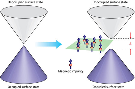
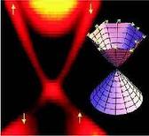
Topological electronic devices
The emerging research field of topological insulator is growing rapidly. Spin orbital coupling (SOC) is the crucial ingredient for a material to be a topological insulator. Driven by the strong spin-orbital coupling, band inversion between two orbitals with opposite parity leads to the helical gapless states crossing the bulk bandgap. Moreover, the spin up electrons and spin down electrons in the gapless states experience opposite effective magnetic field and flow in opposite directions along the boundary, exhibiting quantum spin Hall effect which has attracted great attention in possible spintronics applications. We plan to understand the electronic structures of topological insulator as well as their phonon dispersion relation using the sophisticated approaches, such as tight-binding approach and density functional theory, in order to capture their intrinsic material properties appropriately. We will deeply investigate the effect of doping, vacancy, interface, strain and contact on the electronic structures of topological insulator. Next, we will develop the universal approach based on quantum transport theory to investigate the electron and phonon transport properties in the topological insulator.
(Image: Nano Digest and Science)
Related Publications:
|