Optical MEMS have been conceptualized for a large range of applications, with increasing interest devoted on raster scanning for two-dimensional (2-D) image display. With a number of advantages, including small size, light weight and fast speed compared to conventional bulky scanners, MEMS scanners have been drawing attention for a variety of applications such as heads-up display and picoprojection. The ability of MEMS scanner to display a much bigger multimedia in the forms of images, movies or presentations on an ordinary surface e.g. a wall or a table is fast attracting attention from a wide range of markets, ranging from consumer electronics to automobile.
In the case of the petrochemical industry, sensors deployed during petroleum extraction play important roles in measurement, logging and monitoring of the environment. The cumbersome procedure of extracting and analyzing samples from thousands of feet deep in the earth is expensive and time consuming. One of the possibilities of improving the efficiency is to develop a chemical sensor to detect the content of interest, especially hydrocarbon gas.To ensure a safe working environment, non-dispersive mid-IR gas-sensing system is often used in the measurement of the concentrations of hazardous or combustible gases. The essential component of a NDIR gas-sensing system includes a mid-IR radiation source, a waveguide (often used not only to collimate the light beam, but also as a gas sampling chamber), and an IR detector (often fitted with filters if the IR source is broadband). MEMS will be the core technology to realize such a handheld system consisting of an advanced microsensors-on-a-chip for multi-gas sensing.
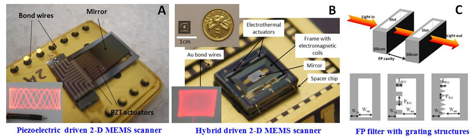
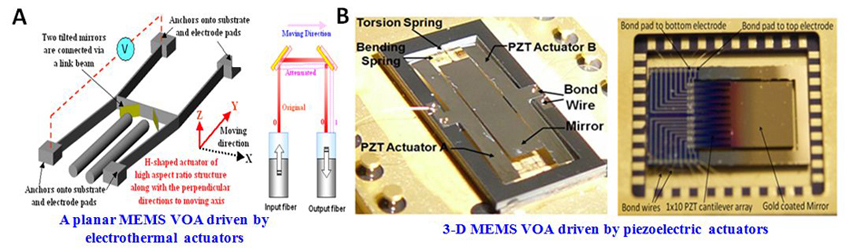
Since the late 90’s, the telecommunication market has attracted enormous investment on optical microelectromechanical systems (MEMS) technology as it has been recognized as an indispensable technology to fulfill a missing link that connects other existing technologies to form an all-optical communication network. Among these optical communication applications, VOA and its array are crucial components for enabling the advanced optical network. Currently, VOAs are adopted to groom power levels across the DWDM spectrum, which help minimize crosstalk and maintain the desired signal noise ratio. In the past few years, our research group has demonstrated various designs of MEMS variable optical attenuators (VOAs) driven by electrostatic, piezoelectric, electromagnetic, and electrothermal actuation.
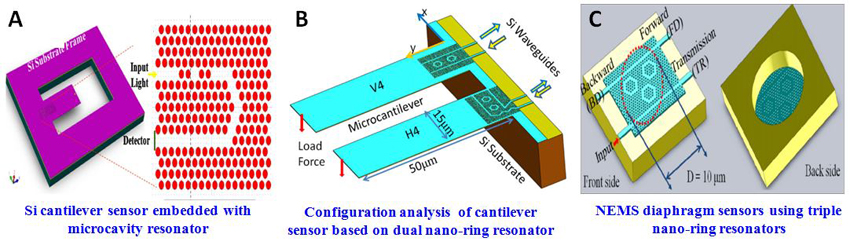
Photonic crystals (PCs) have found important applications ranging from lasers, waveguides, filters, modulators to sensors. In two-dimensional (2-D) PCs, resonant cavity structures can be created by introducing point and/or line defects into the 2-D PC periodic holes array in which it supports field localization in photonic bandgap. Thus PC resonators exhibit resonant wavelength peak which is a function of the surface state of the defects or the shape and dimension of defects in the PC resonant cavity structures. By designing structures of such minute sizes, many interesting phenomena have been demonstrated and examined. In particular, we have shown from our research activities that photonic crystals exhibit much potential to be an important driving force in the near future.
Nanophotonics is the study of the behavior of light on the nanometer scale, and of the interaction of nanometer-scale objects with light. Nanophotonics can provide high bandwidth, high speed and ultra-small optoelectronic components and has the potential to revolutionize telecommunications, computation and sensing. In our group, we investigate plasmonic metamaterials and guided wave in-plane photonics as the platforms of nanophotonics at infrared and mid-infrared spectrum.
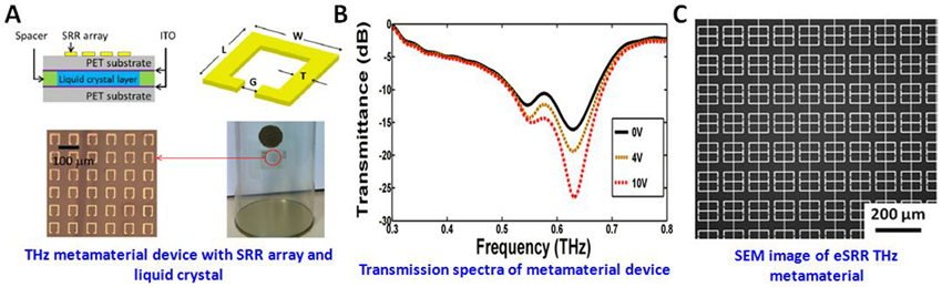
Metamaterials have attracted intense interest for advanced applications in wide areas. Recent works on metamaterials have been extended to the terahertz (THz) frequency range, which result in new potential applications. Tunable THz metamaterials have also received significant attention because of their applications in optical communications, sensing and spectroscopy. Various methods have been proposed and demonstrated to tune the resonant frequency of a metamaterial. Among these methods, geometrically changing the metamaterial unit cells by using MEMS actuators or changing the refractive index of the metamaterial using liquid crystals are some of the research areas that we are undertaking.Our group utilize MEMS technology to explore the possibility of active control of THz metamaterial and their sensing potential.

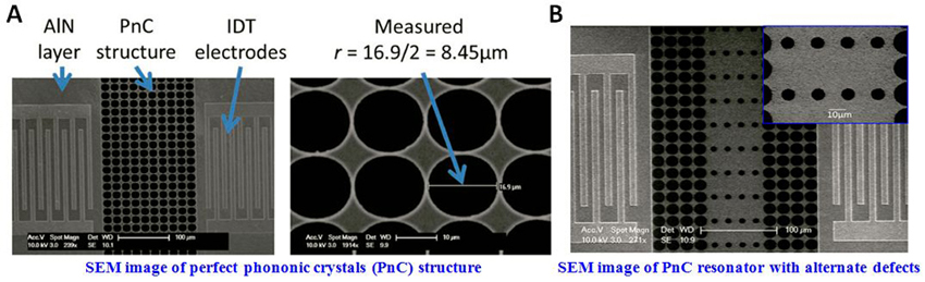
Frequency reference oscillator is one of the key components in current radio-frequency (RF) communication devices, with quartz crystal being widely employed as the oscillator medium. However, due to its intrinsic incompatibilities in many aspects, a much better solution is needed. Among all the possible candidates, silicon-based integrated micromechanical oscillators receive the most attention from the researchers in the related fields because of their advantage such as monolithic integration with integrated circuits. Capacitive-based and piezoelectric-based micro-resonators are the two subtypes of silicon-based integrated micromechanical oscillator. High f-Q product and low motional impedance have yet been realized at the same time for either type. To overcome this trade-off and to achieve high f-Q product with low motional impedance simultaneously are of great scientific and commercial value. Phononic crystals (PnCs), constituted by a periodical repetition of inclusions in a matrix background, is a potential candidate that we are currently researching on, which will overcome the aforementioned trade-off between Q factor and motional impedance.
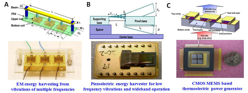
Power MEMS & energy harvesters have been developed to recharge the battery and extend the lifetime of implantable biomedical devices, wireless sensor nodes and devices operating in harsh environment. Harvesting body heat and converting these heat energy into electrical energy is one of the several promising approaches of extending the lifetime of these devices. Other approaches of energy harvesting also include collecting and converting energy from vibrations, i.e. clean and continuous energy sources. There are three kinds of energy transduction mechanisms which generate electricity from vibration, namely electrostatic, electromagnetic and piezoelectric mechanisms. Thermoelectric power generators and vibration-based energy harvesters are currently the two research areas that our group are familiar with.
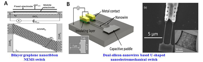
The aggressive scaling of complementary metal oxide semiconductor devices into the sub-100 nm region has resulted in increased short channel effects and gate oxide leakage, which causes a larger power dissipation and unsatisfactory device performance. In recent years, nanoelectromechanical systems (NEMS) have been intensively studied as a promising solution for future low power logic switches and nonvolatile memory applications due to their attractive characteristics such as abrupt switching and an extremely low OFF-state leakage current. However, current NEMS based switches suffer from a high activation voltage, low ON-state current, and large static friction, also known as stiction, which can lead to device failure. New approaches, in the form of material choices and structure designs, are currently undertaken by our research group to overcome the shortcomings of existing NEMS switch..
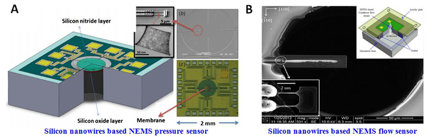
An implantable medical device is considered to be any device that is intended to perform functions inside the body. Implantable microfabricated sensors are, for example, used to facilitate diagnosis or to provide a mean to generate closed loop therapy control. Various kinds of implantable medical devices such as intra-ocular pressure sensor, accelerometer in modern pacemakers have already been implemented in clinical trials. Such an area of research is especially important when we take into consideration of the rapid growth in the different kinds of medical applications in Singapore, particularly during the last decade. As such, we have also diverse our resources and begin making research headway on some of the important biomedical applications using MEMS/NEMS technology.
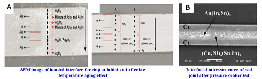
The packaging of MEMS devices is one of the most challenging obstacles to MEMS commercialization. MEMS devices typically comprise of cavities, free-standing or even out-of-plane microstructures, while integrated circuits (ICs) do not. Due to this major difference in nature between MEMS and IC, packaging for MEMS must give space for actuator movement, allowing the sensing element to interact with the surroundings via a pathway, or provide a suitable ambient inside package to achieve higher sensitivity or better reliability. By adopting similar fabrication process flow and CMOS compatible materials such as Cu/Ni/Au metallization, such low temperature wafer bonding techniques also allows for 3D IC integration and extension of Moore's Law, hence creating a new generation of tiny but powerful devices.
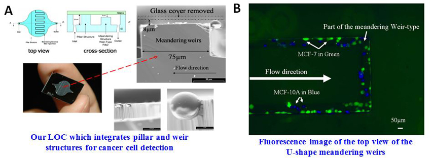
The objective of this project is to develop disposable and practical lab-on-chip (LOC) devices for a continuous flow, highly sensitive separation and detection of tumor cells in whole blood samples. Our LOC device will aim to detect even a few circulating tumour cells (CTCs) of epithelial origin inside the bloodstream in real-time, thus enabling the adoption of a suitable cure before any remarkable metastatic process occurs.
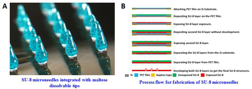
With advances in engineering technology and nanomaterials, scientists now have access to many new and intriguing nanostructures composed of a variety of materials. Nanotubes have become a hot topic in the area of drug delivery because of their high strength and ability to carry molecules both on the outsides and insides. Meanwhile, despite our progress in medical technology, the needle is still almost exclusively used as a vaccine delivery device. The use of needles canlead to serious distress in children, and indoctrinates us with a negative view of doctors and health care that can last a lifetime. Platforms to spare people the needle are seriously lacking, or they still have pain associated with their delivery. The goal of our research here is to leverage the strength of nanotubes to penetrate the skin and deliver vaccines painlessly through the first few layers of skin.
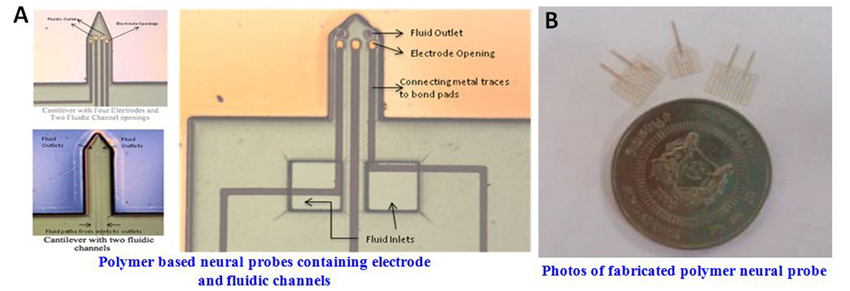
This project aims to establish new capabilities in Singapore in developing neuroprosthetic devices. More specifically, the new capabilities will involve advancing neural stimulation and recording techniques through micro/nano technologies. The techniques proposed here are in line with the theme of the TSRP and accordingly at the interface of biology (neural or neuromuscular tissue), micro/nano neural electrodes (MEMS/NEMS), and electronics (stimulation waveform generation, low-noise recording amplifiers and signal processing). In consideration of the rapid growth in medical applications, Singapore shall expand its research base for neural interfacing so as to harvest a research ecosystem suitable for this industry sector to anchor in the region.
T-CRP |
|||||
|---|---|---|---|---|---|
| Programme Title | Programme PI | Award No. | S4H WBS No. | Total Awarded Amount (SGD) | Duration of Project |
| Electrostatic/Piezoelectric Hybrid-Actuated CMOS-compatible Nano Optomechanical Building Blocks and Technology Platform for Next-Generation Optical IoT Sensing / Communication Systems | Prof. Chengkuo Lee | T-CRP-2025-0009 | A-8004170-00-00 | 1,989,000 | 01/02/2026 to 31/01/2030 |
Frontier CRP |
|||||
| Programme Title | Programme PI | Award No. | S4H WBS No. | Total Awarded Amount (SGD) | Duration of Project |
| CMOS Photonics Platform for Next Generation Photonics AI Engines | Prof. Chengkuo Lee | NRF-F-CRP-2024-0006 | A-8003247-00-00 | 1,994,200 | 01/04/2025 to 31/3/2028 |
CRP-28th |
|||||
| Programme Title | Lead PI | Proposal Number | Total Awarded Amount (SGD) | Duration of Project | |
| Intergrating Wideband Tuneable Acoustic Filters on Silicon for High-Speed Wireless Communication | Dr. Huajun Liu | NRF-CRP28-2022-0002 | 9,641,360 | 04/01/2023 to 03/31/2028 | |
| Sub-Project Title | PI | S4H WBS No. (New) | Total Awarded Amount (SGD) | Duration of Project | |
| Acoustic Filters | Prof. Chengkuo Lee | A-8001503-00-00 | 3,004,762 | 04/01/2023 to 03/31/2028 | |
CRP-15th |
|||||
| Programme Title | Programme PI | ECC WBS No. (Old) | S4H WBS No. (New) | Total Awarded Amount (SGD) | Duration of Project |
| Piezoelectric Photonics Using CMOS Compatible AlN Technology for Enabling The Next Generation Photonics ICs and Nanosensors | Prof. Chengkuo Lee | R-263-000-C24-281 | A-0005947-20-00 | 6,074,816 | 01/07/2016 to 31/12/2021 |
CRP-10th |
|||||
| Programme Title | Programme PI | Proposal Number | Total Awarded Amount (SGD) | Duration of Project | |
| Peripheral Nerve Prostheses: A Paradigm Shift in Restoring Dexterous Limb Function | Prof. Nitish V. Thakor | NRF-CRP10-2012-01 | 9,949,798 | 01/01/2014 to 31/12/2018 |
|
| Sub-Project Title | PI | Project Number | Total Awarded Amount (SGD) | Duration of Project | |
| Neural Interface | Dr. Chengkuo Lee | R-719-000-001-281 | 2,220,140 | 01/01/2014 to 31/12/2018 | |
CRP-08th |
|||||
| Programme Title | Programme PI | Proposal Number | Total Awarded Amount (SGD) | Duration of Project | |
| Self-Powered Body Sensor Network for Disease Management and Prevention Oriented Healthcare | Prof. Lian Yong | NRF-CRP8-2011-01 | 9,929,814 | 01/10/2012 to 30/09/2017 | |
| Sub-Project Title | PI | Project Number | Total Awarded Amount (SGD) | Duration of Project | |
| Energy Harvesting Solutions for Biosensors | Dr. Chengkuo Lee | R-263-000-A27-281 | 2,336,200 (Budget awarded to PI: 1,954,000) | 01/10/2012 to 30/09/2017 | |
NRF MID-SIZED CENTER GRANT |
|||||
|---|---|---|---|---|---|
| Programme Title | Lead PI | Proposal Number | Total Awarded Amount (SGD) | Duration of Project | |
| National Centre for Advanced Integrated Photonics (NCAIP) | Prof. TJIN Swee Chuan | NRF-MSG-2023-0002 | 2,983,100 | 16/04/2024 to 15/04/2031 | |
| Sub-Project Title | PI | S4H WBS No. (New) | Total Awarded Amount (SGD) | Duration of Project | |
| Integrated Photonics Platforms | Prof. Chengkuo Lee | - | A-8002837-02-00 (for EOM); A-8002837-00-00 (for OOE) | 16/04/2024 to 15/04/2031 |
RIE 2025 - INDUSTRY ALIGNMENT FUND – INDUSTRY COLLABORATION PROJECTS (IAF-ICP)
|
|||||
|---|---|---|---|---|---|
| Programme Title | Programme PI | Grant No. (for acknowledgement) | Total Awarded Amount (SGD) | Duration of Project | |
| Piezo Specialty Lab-in-Fab 2.0 (LiF 2.0) – Enabling Unrivalled Power Efficient Transducers Beyond Material Limits | Dr. Yao ZHU | I2301E0027 | 70,049,473 | 15/02/2024 to 14/02/2029 | |
| Sub-Project Title | PI | S4H WBS No. (New) | Total Awarded Amount (SGD) | Duration of Project | |
| Ultra power efficient MEMS transducers | Prof. Chengkuo Lee | A-8002231-00-00 | 2,195,750 | 15/02/2024 to 14/02/2029 | |
RIE2020-AME-2019-Nanosystems at the Edge |
|||||
| Programme Title | Programme PI | Grant No. (for acknowledgement) | S4H WBS No. (New) | Total Awarded Amount (SGD) | Duration of Project |
| Nanosystems at the Edge | Dr. Eldwin Ng Jia Qiang | A18A4b0055 | 21,872,340 | 01/03/2019 to 29/02/2024 | |
| Sub-Project Title | PI | ECC WBS No. (Old) | S4H WBS No. (New) | Total Awarded Amount (SGD) | Duration of Project |
| Ultra-Low-Power Physical Sensors | Dr. Chengkuo Lee | R-263-000-D67-305 | A-0005111-03-00 | 1,438,920 | 01/03/2019 to 29/02/2024 |
RIE2020-AME-2019-BRENAIC |
|||||
| Programme Title | Programme PI | Grant No. (for acknowledgement) | S4H WBS No. (New) | Total Awarded Amount (SGD) | Duration of Project |
| BRain-Efficient Nanomechanical Artificial Intelligence Computing (BRENAIC) | Dr. Nan Wang | A18A5b0056 | 22,236,588 | 07/03/2019 to 06/03/2024 | |
| NUS PI | ECC WBS No. (Old) | S4H WBS No. (New) | Total Awarded Amount (SGD) | Duration of Project | |
| Dr. Chengkuo Lee | R-263-000-D78-305 | A-0005117-02-00 | 2,683,400 | 07/03/2019 to 31/12/2022 |
| Title of Supported Project | Funding Body | Role in Supported Project | Award No. | S4H WBS No. | Total Funding / Awarded Amount (SGD) | Duration of Project |
|---|---|---|---|---|---|---|
| Advanced Photonic AI Chips for Robust Predictions of Stochastic Process Using Photonic Bayesian Neural Networks | Ministry of Education (MOE) | PI | T2EP50125-0030 | A-8004456-00-00 | 720,850 | 2/21/2026 to 2/20/2029 |
| Electro-Optic (EO)-Enhanced Memory on Lithium Niobate Integrated Platforms | Microelectronics Seed Grant Funding | PI | - | A-8003551-00-00 | 250,000 | 7/1/2025 to 6/30/2028 |
| A Multimodal Sensing/ Haptic System Forlower-Limb Exoskeleton Feedback Control | NUS College of Design and Engineering (CDE) – Robotics Seed Grant Programme | Team PI | - | A-8003281-00-00 | 249,000 | 3/17/2025 to 3/16/2028 |
| AI-Sensor Enhanced Medical Operation Training System | NUS College of Design and Engineering (CDE) – Robotics Seed Grant Programme | Team PI | - | A-8003283-00-00 | 249,800 | 3/17/2025 to 3/16/2028 |
| Wearable Exoskeleton/Exosuit Systems Enhanced by Flexible Electronics, Haptic Technology and Cloud AI for Sports and Rehabilitaion Applications | Research Platfirm for biomedical and Health Techonolgy (RP-BHT, NUSRI) | PI | - | - | 1,800,000(RMB) | 01/09/2024 to 31/12/2028 |
| National Semiconductor Translation and Innovation Centre (NSTIC) | MTC RIE2025 | Team PI | M24W1NS005 | A-8002323-00-00 | 748,800 | 01/05/2024 to 30/04/2029 |
| Title of Supported Project | Funding Body | Role in Supported Project | Project Number | Total Awarded Amount (SGD) | Duration of Project |
|---|---|---|---|---|---|
| Chip-scale Multispectral 3D Scanner (CMUS) | MTC IAF-PP | Team PI | M23M5a0069 | 4,980,261 / 520,000 | 01/03/2024 to 28/02/2027 |
| Terahertz Reconfigurable Intelligent Metasurfaces (TRIM) for 6G communications | MTC Programmatic Funds | Team PI | M22H1b0110 | 11,229,790/650,000 | 01/03/2023 to 28/02/2026 |
| Reseach and design of a MEMS interruptor module | DSO National Laboratories | PI | - | 800,800.00 | 31/08/2022 to 30/05/2025 |
| Artificial Intelligence Circuits of Hybrid Integrated Photonics System (AI CHIPS) | Ministry of Education (MOE) | PI | NUS WBS: R-263-000-F18-112 | 743,640 | 01/11/2021 to 31/10/2024 |
| Under-utilised Potential of Microbiomes (soil) in Sustainable Urban Agriculture | Reimagine Research Scheme (RRSC) | PI | NUS WBS: R-263-000-F11-114 (OD | 82,249.98 | 15/09/2021 to 14/03/2024 |
| Scalable AI Phenome Platform towards Fast-Forward Plant Breeding (Sensor) | Reimagine Research Scheme (RRSC) | PI |
NUS WBS: R-263-001-E75-114 (ODPRT) R-263-001-E75-114 (FOE) |
406,700 | 31/03/2021 to 30/03/2024 |
| AI-assisted Infrared Nano-Opto-Surface Enhanced-Sensor (IR-NOSES) Chips for Early-stage Diagnosis and Healthcare Applications | Advanced Research and Technology Innovation Centre (ARTIC) | PI |
NUS WBS: R-261-518-009-720 |
394,000 | 10/10/2020 to 09/10/2023 |
| Intelligent Monitoring System Based on Smart Wearable Sensors and Artificial Technology for the Treatment of Adolescent Idiopathic Scoliosis | NUS iHealthtech Grant: Smart Sensors and Artificial Intelligence (AI) for Health | PI |
S4H WBS NO. A-0005180-16-00 | 100,000 | 01/08/2020 to 31/07/2022 |
| Advanced Wearable Glucose and Gas Sensors Based on Hybrid Detetcion Mechanism by Leveraging Plasmonic Nano-Antennas | Ministry of Education (MOE) | PI |
S4H WBS NO. A-0005138-01-00 | 50,000 | 16/10/2019 to 15/10/2022 |
| Explainable AI as a Service for Community Healthcare | AISG | Co-PI |
Grant No. AISG-GC-2019-002 | 4,999,520 | 01/05/2019 to 30/04/2021 |
| Chip-Scale MEMS Micro-Spectrometer for Monitoring Harsh Industrial Gases | A*STAR-NCBR | PI |
NUS WBS: R-263-000-C91-305 | 300,000 | 01/11/2017 to 30/04/2021 |
| Reconfigurable data center optical interconnects using fast nanophotonic MEMS waveguide switches | NRF-ISF | PI |
NRF2015-NRF-ISF001-2620 NUS WBS: R-263-000-C64-281 | 422,400 | 16/03/2017 to 15/03/2021 |
| Fast Prototyping of Smart Toilet IoT Sensor System Using 3D Printing | NAMIC | PI |
NUS WBS: R-263-000-E54-592 | 24,000 | 01/08/2020 to 31/01/2021 |
| Hybrid Integration of Flexible Power Source and Pressure Sensors | HIFES Seed Funding-2017-01 | PI |
NUS WBS: R-263-501-012-133 | 393,000 | 01/04/2017 to 30/11/2019 |
| THz Metamaterial Based Microemitters (Title in Chinese: 微型化亚太赫兹超材料发射器的研究) | National Natural Science Foundation of China | PI |
Grant No. 61474078 | 182,000(RMB 850K) | 01/2015 to 12/2018 |
| Thermoelectric Power Generator (TEG) Based Self-Powered ECG Plaster - System Integration (Part 3) | NUS;FRC | PI |
NUS WBS: R-263-000-B56-112 | 179,999 | 01/03/2015 to 28/02/2018 |
| Monolithic integrated Si/AlN nanophotonics platform for optical NEMS and OEICs | MOE/NUS; ARF-Tier 2 | PI |
MOE2012-T2-2-154 NUS WBS: R-263-000-A59-112 | 612,358 | 22/07/2013 to 21/07/2016 |
| Development of Wearable Micro Blood Flow Sensors for Livestock Breeding | A*STAR-JST 2nd Joint Grant Call | PI |
SERC: 1220103064 NUS WBS: R-263-000-A56-305 |
233,667 | 21/01/2013 to 20/01/2016 |
| MEMS Energy Harvesting Mechanisms for Collecting Energy from Vibrations | MOE/NUS; FRC | PI |
WBS: R-263-000-692-112 |
163,000 | 01/03/2012 to 28/02/2015 |
| Novel Sensors and Acoustic Transducer for the Down-hole Electronic System | A*STAR, SERC, Rugged Electronics Programme | PI |
SERC: 1021650084 NUS WBS: R-263-000-643-305 |
965,040 (Budget awarded to ECE: 804,200) | 08/02/2011 to 07/02/2014 |
| Development of NEMS switch with CMOS compatible process technology for next-generation IC applications | A*STAR, SERC, PSF | PI |
SERC: 1021010022 NUS WBS: R-263-000-612-305 |
964,668 (Budget awarded to ECE: 803,890) | 01/08/2010 to 31/01/2014 |
| Nanoneedle Devices for Transdermal Vaccine Delivery | MOE/NUS; ARF-Tier 2 | Co-PI | MOE2009-T2-2-011 WBS: R-263-000-598-112 | 1,040,630 (Budget awarded to ECE: 512,510) | 01/06/2010 to 31/08/2013 |
| Peripheral Nerve Recording and Muscle Simulation | A*STAR, SERC, TSRP-Integrated Nano-Photo-Bio-Interface (iNPBi) | Co-PI | SERC: 1021520013 WBS: R-263-000-601-305 | 1,254,528 (Budget awarded to ECE: 581,830) | 01/05/2010 to 31/10/2013 |
| Integration of Si photonic crystals and MEMS actuator for next generation active and tunable nanophotonics in filter and modulator applications | A*STAR, SERC, PSF | Co-PI | SERC: 0921010049 | 826,830 (Budget awarded to ECE: 689,025) | 01/09/2009 to 28/02/2013 |
| Bionic Neural link for nerve function restoration | MOE/NUS; FRC | Co-PI | WBS: R-263-000-533-112 | 150,000 | 01/03/2009 to 31/12/2011 |
| Development and Integration of 2D Si Photonic Crystals Nanodevices with Nanofluidics and BioMEMS for Biomedical Sensing Applications | MOE/NUS; URC-Tier 1 | PI | WBS: R-263-000-475-112 | 250,000 | 21/01/2008 to 22/07/2011 |
| Si MEMS (Microelectromechanical Systems) based energy harvesters for wireless medical sensor nodes | A*STAR SERC National Home 2015 Programme | PI | SERC: 0621150043 | 225,288 | 15/04/2007 to 14/04/2009 |
| Low temperature wafer bonding | A*STAR, IME | PI | IME: 06-42004 | 244,000 | 24/12/2006 to 30/12/2008 |
| Development of novel variable optical attenuators | MOE/NUS; FRC | PI | WBS: R-263-000-358-112/133 | 174,150 | 01/01/2006 to 30/06/2009 |
Chengkuo Lee group
Electrical and Computer Engineering
National University of Singapore
4 Engineering Drive 3
Singapore, 117583
+65 6516-5865