Research Facilities
Centre for Optoelectronics have three cleanrooms (one class 1000 and two class 10,000) with microelectronics device processing equipments, facilities and state-of-art material growth facilities. The center's facilities, expertise and continuing research efforts would enhance the capability of the Centre to produce a wider range of Optoelectronics devices and Nano-photonics technology.
Equipment / Facilities Usage
Equipment Registration User Guides
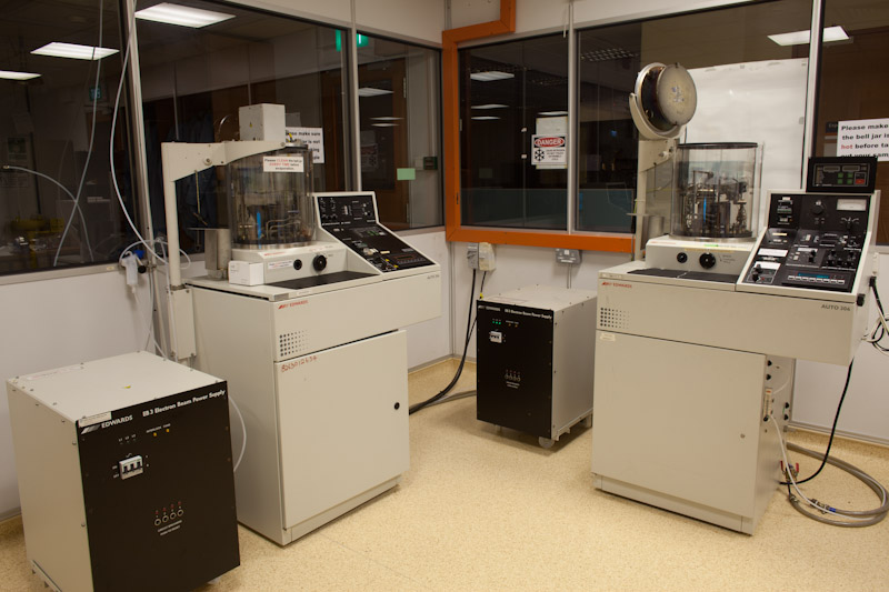
Electron Beam Evaporation System (2 units) |
|
|
|
Super User: Musni
Edward E-beam evaporation system for Metal Deposition
Model: Edward Auto 306 Turbo
Substrate size: irregular to standard 8”dia wafer |
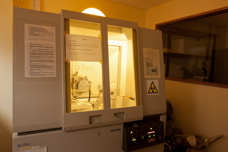
High Resolution Double Crystal X-Ray Diffractometer |
|
|
Super User: Rayson Tan (IMRE)
X-pert Pro-MRD, PW 3050/65 X-ray diffractometer
Model: X-pert Pro-MRD, PW 3050/65
X-Ray source: Cu
X-Ray Optics: (Incident beam optics) Ge(220) with mirror for 4 bounce high-resolution and high intensity, (Diffracted beam optics) Soller slits/collimators/monochromator. |
Inductively Coupled Plasma Etching System (ICP) |
|
|
Super User: Son Jae Sung
Plasma-Therm Inductively Coupled Plasma Etching System (ICP)
Model: SLR Series (SLR-770)
Substrate size: irregular to standard 8”dia wafer |
I-V Probe station |
|
Super User: Musni
Model: Micromanipulator-Model 6000 with Temperature-Variable Chuck
X-Y stage: moves 4"x4", chuck is for low contact resistance. The operating temperature can be varied from room temperature to 400*C.
Model: Parameter Analyzer B1500A with 1 High Power SMU (HPSMU), 2 Medium Power SMUs (MPSMU), 1 MFCMU and 1 GNU.
Capabilities: I-V measurement (1pA-1A), Pulsed I-V measurement, C-V measurment (frequency up to 1MHz). Windows OS-Based Software. |
|
Laser Writer |
|
|
Super User: Zhang Chi
Model: Microtech Laserwriter LW405-A
Substrate size: up to 150x150 (6”x6”) (mm) Variable resolution: In the Laser Writer system the resolution is changed by replacing the beam focusing optics, which takes only a few seconds |
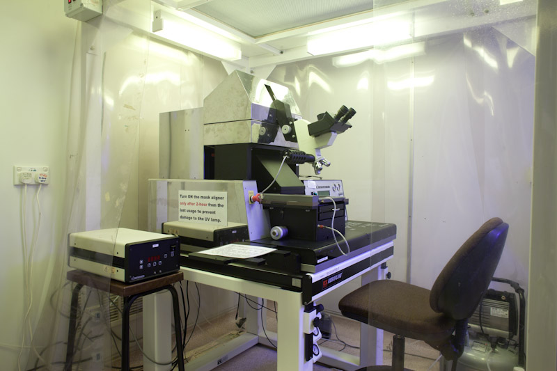
Mask Aligner |
|
|
Super User: Musni
Model: Karl Suss MA6
|
Metal Organic Chemical Vapor Deposition System (AIXTRON) |
|
|
Super User: Chia Ching Kean (IMRE), Terry Zhuo (IMRE), Jin Yunjiang (IMRE)
AIXTRON 200/4 MOCVD system for III-V (Arsenide, Phosphite) material growth research
MO Sources:
Reactor:
|
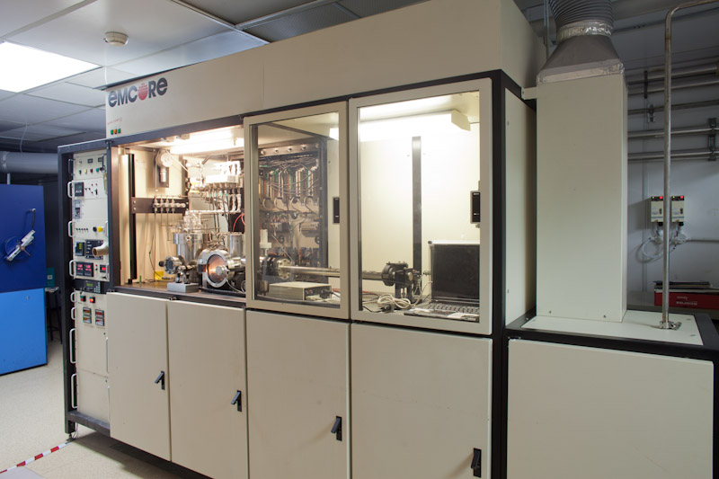
Metal Organic Chemical Vapor Deposition System (Emcore) |
|
|
Super User: Rayson Tan (IMRE), Soh Chew Beng (IMRE), Zhang Li
EMCORE D-125 MOCVD system for III-V (Nitride) Material growth research
MO Sources:
Reactor:
|
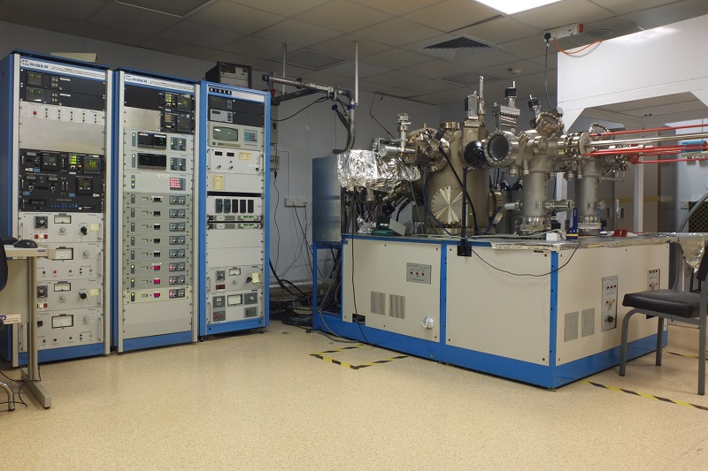
Molecular Beam Epitaxy (MBE) System |
|
|
Super User: Tung Kar Hoo, Patrick
RIBER 32P MBE system for III-V (Arsenide-based) material growth research
The MBE system can growth III-V semiconductors In(Al or Ga)As(N) Epitaxial Source Materials: In, Ga, Al, and As cracker cell. Doping Materials: Si, Be |
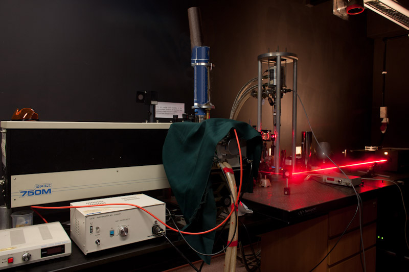
Photoluminescence Optical Characterization (Low-temp) |
|
|
Super User: Musni
Low-temp Photoluminescence setup
Laser Sources:
|
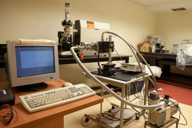
Photoluminescence Optical Characterization (Micro) |
|
|
Super User: Tay Chuan Beng
Micro-Photoluminescence Measurement
Hardware setup based on Renishaw Ramascope 2000
|
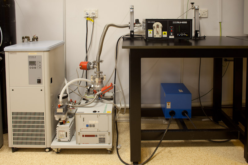
Rapid Thermal Annealing System (2 units) |
|
|
Super User: Musni
ULVAC Rapid Thermal Annealing System
Model: Mila-3000
Max size: less than (20 x 20) mm |
Surface Profiler |
|
|
Super User: Musni
Model: Alpha Step 200 (Tencor Instrument, USA)
Vertical sensitivity: Measures the small steps - 20 to 50Å |