End-point Monitoring and Control of Photoresist Development Process
Motivations and Objectives
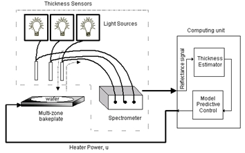
In-situ measurement of film thickness during the development and etching process is important for process control, on-line diagnostics and real-time feedback control. Photoresist linewidth are affected by many factors such as resist film thickness, solvent content, exposure dose, etc. Drift in other process variables may cause the optimized development time to vary. If during development, the exposed film thickness is monitored by the optical detection of interference fringes, it is possible to find the time at which the photoresist breaks through to the substrate ("end point"). This time is related to the total development time needed to print a given feature size, it is possible to automatically adjust the total time to correct for process drifts in dose, resist thickness or softbake temperature and reduce linewidth variation.
One of the main objectives of the multi-wavelength DRM is to develop a robust endpoint detector to determine the end of development process. The reflectivity measurements from the DRM provide a diagnostic capability as it provides a window into the resist film's dissolution profile. A study of the differences between development signals can reveal such processing problems such as resist lifting, scumming, and overbaking. The ability to monitor the wafer development also gives independent confirmation that the process is unchanging from wafer to wafer. Besides wafers, the DRM can also be used to obtain the correct critical dimension on photomask substrate. Studying the uniformity of development in the inspection area can optimize critical dimension uniformity.
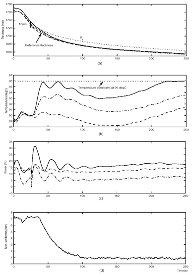
Another application made possible with the setup is the possibility of controlling the photoresist thickness during the softbake process.
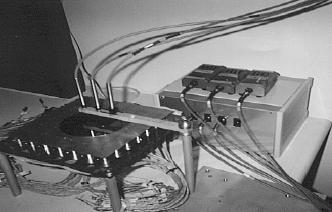
Hardware Setup
Model Predictive Control