Magnonics 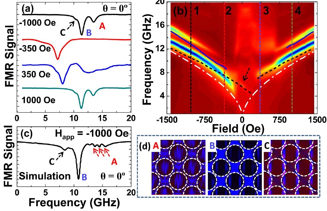 Recently, there has been growing interest in the fundamental understanding of spin wave (SW) propagation in magnonic crystals (MC), which are coupled periodic magnetic nanostructures conceived as the magnetic analogue of photonic crystals. This interest is largely due to advances in lithography and other controlled nanofabrication techniques, the development of new experimental techniques for studying high-frequency magnetization dynamics and the potential use of spin waves as information carriers in spintronic applications. Recently, there has been growing interest in the fundamental understanding of spin wave (SW) propagation in magnonic crystals (MC), which are coupled periodic magnetic nanostructures conceived as the magnetic analogue of photonic crystals. This interest is largely due to advances in lithography and other controlled nanofabrication techniques, the development of new experimental techniques for studying high-frequency magnetization dynamics and the potential use of spin waves as information carriers in spintronic applications.
A SW can be considered as a magnetic analogue of a sound or light wave. The wavelength of SWs is several orders of magnitude shorter than that of electromagnetic waves; therefore magnonic crystal based devices offer better prospects for miniaturization in the gigahertz to terahertz range. In addition, magnonic devices are made from non-volatile memory elements, and therefore, their integration will enable programmable devices with ultrafast re-programming at the sub-nanosecond time scale. It has been predicted theoretically that the frequency spectrum of MC will consist of bands of allowed magnonic states and forbidden frequency gaps analogous to what has been observed in photonic crystals. One of the main challenges is to fabricate high quality periodic magnetic nanostructures. My group has been focusing on the design and optimization of high quality bi-component magnonic crystals including band gap parameters.
- We are systematically investigating the dynamic properties of magnonic crystals of macroscopic macrosizes comprised of nanoscale features using broadband ferromagnetic resonance spectroscopy in the frequency range from 40 MHz to 40 GHz. This broadband FMR system incorporating a probe station was developed in my group. In contrast to conventional FMR, where a microwave cavity (limited to a single resonance frequency) is used, a coplanar waveguide (CPW) is used in our broadband FMR to create the oscillating field which excites the magnetization precession with easily detectable amplitude in a broad range of frequencies.
- We are also probing the magnetization dynamics of individual microscopic nanostructures [otherwise the difference with the preceding item is not very clear], by using electron beam lithography to define single elements on top of CPW connected to a vector network analyzer (VNA) by microwave probes. This is followed by the measurement of the scattering parameters (transmission and reflection coefficient).

Further readings:
- J. Ding, M. P. Kostylev, and A. O. Adeyeye, Phys. Rev. Lett., 107,047205 (2011).
- J. Ding, M. P. Kostylev, and A. O. Adeyeye, Phys. Rev. B, 84,054425 (2011).
- Z. K. Wang, V. L. Zhang, H. S. Lim, S. C. Ng, M. H. Kuok, S. Jain and A. O. Adeyeye ACS-Nano Vol 4, 643 (2010).
- Z. K. Wang, V. L. Zhang, H. S. Lim, S. C. Ng, M. H. Kuok, S. Jain and A. O. Adeyeye Applied Physics Letters 94,083112 (2009).
- S. Jain and A. O. Adeyeye , Applied Physics Letters 94, 062510 (2009)
|