An introduction to the empirical pseudopotential method
Aaron J. Danner
Created
at the
Last edited on January 31,
2011
Abstract: Using
some of the first published papers from the 1960’s on the pseudopotential
method, a program was completed which allows fully vectorial
electronic band structure calculations on diamond and zincblende
materials, including Si and GaAs. This article introduces the pseudopotential method from first principles and
illustrates its use with Si, GaAs, and
1. Useful downloads
E-mail me if you would like a copy of the Mathematica program (ask me for the pseudopotential.nb file). The school's web security settings prevent me from linking to it directly. Left click to go to the download site for MathReader, free software which allows Mathematica code to be viewed for study even if Mathematica is not installed.
I also have a MathCad implementation generously provided by Mr. Pierre Tomasini (ask me for the Mathcad_Tomasini.pdf file) of Arizona State University.
2. Introduction
The
empirical pseudopotential method was developed in the
1960’s [1-3] as a way to solve Schrodinger’s equation for bulk crystals without
knowing exactly the potential experienced by an electron in the lattice. Since electrons are interacting with the
crystal lattice, an electronic band structure calculation is a many body
problem (unlike the situation in photonic crystal calculations, for example
[4]). Although other methods existed at the time for approximating electronic
band structures, the pseudopotential method gives
surprisingly accurate results considering the computing time and effort
involved.
The basic scheme is to assume that the core
electrons are tightly bound to their nuclei, and the valence and conduction
band electrons are influenced only by the remaining potential. Since the potential can be Fourier expanded
in plane waves, an eigenvalue equation for
determining an E-k relationship can be established. Although the Fourier coefficients for the
potentials are not known, they can be empirically determined for a given
crystal by fitting calculated crystal parameters to known measurements. Cohen and Bergstresser
followed these steps to determine band structures of several diamond and III-V zincblende structures [5].
In this term paper, I repeat the original steps
taken by Cohen and Bergstresser in formulating the pseudopotential method, then carry out calculations using a
computer program I wrote to construct the electronic band diagrams of Si and GaAs using their form factors. Then, I apply the method to AlAs, for which form factors are essentially unavailable,
and construct a plausible E-k diagram for the compound using known
parameters. Limitations on the method
used are discussed, as well as more powerful methods of determining accurate
band structures.
3. Theoretical basis
This
development is essentially identical to that followed by Cohen and Bergstresser [5] and others [6, 7]. Starting out with the time-independent
Schrodinger equation,
 (1)
(1)
we
use Bloch’s theorem to restate the wavefunctions in
terms of plane waves (because the crystal is a periodic structure).
![]() (2)
(2)
Because
of the periodic nature of both the wavefunction and
the potential, plane wave expansion can be used to write each as an infinite
series, summed over reciprocal lattice vectors.
![]() (3)
(3)
![]() (4)
(4)
In
Equations (3) and (4), the parameters A and V represent Fourier coefficients
for given reciprocal lattice vectors.
Substituting Equations (3) and (4) into the Schrodinger equation, the
result is the following:
![]() (5)
(5)
Equation
(5) is then multiplied by an orthogonal function ![]() and integrated over the
volume of the crystal. This creates Kronecker delta functions where previously there were
exponentials.
and integrated over the
volume of the crystal. This creates Kronecker delta functions where previously there were
exponentials.
![]() (6)
(6)
In Equation (6), one summation in
each term can be eliminated. For
example, in the first term, h and l must be equal in order for
the term to be non-zero. Thus the
summation over h includes only one non-zero term. Likewise, a summation can be eliminated from
each of the other two terms.
![]() (7)
(7)
Equation
(7) can be cast as an eigenvalue equation with the
following matrix form, where H represents the Hamiltonian matrix
element. If the Fourier series were not
truncated, then the matrix would be infinite in size. In calculations that will be carried out
later, it was found that a 124 x 124 matrix resulted in reasonable
accuracy. Reference (6) shows a matrix
only involving positive values of l and h, which seems to be
incorrect. This type of Fourier
expansion should be symmetric about the origin. If this were not the case, then
the eigenvalues would not be guaranteed to be real.
 (8)
(8)
To solve Equation (8), the Hamiltonian matrix must
be diagonalized, which can be accomplished using
standard numerical routines. The eigenvalues of the matrix are the possible values of energy
E(k). For each k
vector in a band diagram, the matrix must be diagonalized.
Equation
(9) allows the calculation of each element in the matrix. The remaining problem is to find appropriate
values for the potential function V.
![]() (9)
(9)
Because there are two atoms per cell in the fcc structure for zincblende or
diamond materials, the potential must include the contribution of both. The convention of Cohen and Bergstresser will be followed, taking the point halfway
between the atoms as the origin of each cell in the fcc
structure. The potential itself can be
split into symmetric and antisymmetric parts, as in
Equation (10),
![]() (10)
(10)
where ![]() represents the absolute offset of an atom from
the origin of each cell in the fcc lattice. (One atom
is located at the cell origin offset by
represents the absolute offset of an atom from
the origin of each cell in the fcc lattice. (One atom
is located at the cell origin offset by ![]() ,
and the other atom is offset by -
,
and the other atom is offset by -![]() .)
For the materials considered here,
.)
For the materials considered here,
![]() (11)
(11)
The terms ![]() and
and
![]() are known as the form
factors, and are usually determined empirically, although there are some first
principles approaches reported [8]. It
has been found that only six terms are necessary for reasonable accuracy, which
eases the task of pinpointing their values empirically. Form factor determination will be discussed
further in the next section. Equations
(1) through (11) represent the local pseudopotential
theory. They were used to create band
diagram software (see Appendix) using Mathematica,
although any language (especially those including linear algebra libraries)
could be used.
are known as the form
factors, and are usually determined empirically, although there are some first
principles approaches reported [8]. It
has been found that only six terms are necessary for reasonable accuracy, which
eases the task of pinpointing their values empirically. Form factor determination will be discussed
further in the next section. Equations
(1) through (11) represent the local pseudopotential
theory. They were used to create band
diagram software (see Appendix) using Mathematica,
although any language (especially those including linear algebra libraries)
could be used.
Although the eigenmatrix can be determined from Equations (9) and (10),
the task of properly ordering the reciprocal lattice vectors correctly in the
matrix can appear daunting. I have created a generating function that can carry
out the task. Because the reciprocal lattice
vectors K are based on the basis reciprocal lattice vectors (i.e. K =
hb1+ kb2+ lb3,
where h, k, and l are integers), care must be taken to ensure
that the three integer variables are properly incremented from the center of
the matrix along the columns so that all states are included and none are
skipped. Refer to the documented source
code in the Appendix, where it is apparent that K can be written as a
function of only matrix row.
4. Application: Si and GaAs band structure calculations
Table 1 shows form factors
as given by Cohen and Bergstresser [5] (except
silicon [9]). These were used as inputs
(along with lattice constant) to the band structure program (Appendix) to
confirm their results. The form factors for Ge have
been included to illustrate the method that was used to originally determine
the form factors for GaAs.
Because
Ge lies between Ga and As
in the periodic table, it is reasonable that its symmetric form factor should
be the same (charge balanced at each fcc cell in the
same way for the symmetric term).
However, because the atoms are no longer the same, there is an antisymmetric term that enters Equation (10). Note that this causes the eigenmatrix
to be complex. Nevertheless the eigenvalues are guaranteed to be real.
Table 1: Form factors found in literature (circa 1965),
given in Rydbergs
|
Form factor |
Si
[9] |
Ge [5] |
GaAs [5] |
|
VS3 |
-0.21 |
-0.23 |
-0.23 |
|
VS8 |
0.04 |
0.01 |
0.01 |
|
VS11 |
0.08 |
0.06 |
0.06 |
|
VA3 |
0 |
0 |
0.07 |
|
VA4 |
0 |
0 |
0.05 |
|
VA11 |
0 |
0 |
0.01 |
The actual
calculation of the energy eigenvalues for a single k
point took less than a minute on a 733 MHz Pentium III machine. I have included
the L, G, X, K, and W symmetry
points in the band diagrams, shown in Figures 2 and 3. The distances along the k axes between
symmetry points were calculated based on the actual distance moved in k
space through the Brillouin zone, which is why, for
example the distance from G to X is much larger than
the distance from X to W. Figures 2 and
3 show good agreement with published band structures [5].
Although the band structures agree almost perfectly with the
original work of Cohen and Bergstresser, they do not
include localized effects or spin-orbit coupling. For example, at the G point in GaAs the
split off band is not lowered correctly.
The reason for this is that the pseudopotential
is not just dependent on the energy, but also on the angular momentum
components from electrons in the core states.
These interactions have been neglected in the above development and can
be included by adding correction terms to the Hamiltonian matrix element [9],
but this is beyond the scope of this term paper.
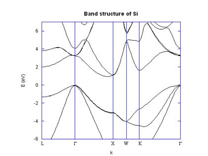
Fig. 1
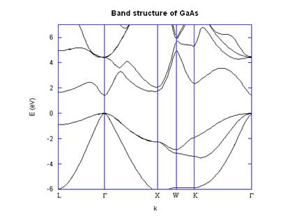
Fig. 2
5. Determination of AlAs
form factors
I was
only able to find form factors for AlAs from one
source (“DAMOCLES”) [7], and using them in a band structure calculation did not
result in the correct energy gaps at symmetry points, as shown in Table 2. The discrepancies should be qualified: DAMOCLES values might be used in more
complicated formulations, where spin-orbit interactions are included as well as
non-local phenomena which could alter the main pseudopotential
terms. However that information was not
available since DAMOCLES data was obtained from an internet site advertising
its capabilities, not necessarily a trusted publication. It is apparent that the base pseudopotentials do change when adding correction
terms. Nonetheless the data quoted in
Table 2 was the only data on AlAs available, except
for a first principles calculation (OPW method) carried out at a time when
little experimental data was available for confirmation [10].
Table 2: Primary gaps from
(a) theoretical IBM project, (b) trusted experimental source,
and (c) my pseudopotential calculation
|
Parameter |
(a)
DAMOCLES
[7] |
(b) Experimental
[8] |
(c) Fitted |
|
EGG |
2.39
eV |
2.991
eV |
2.97
eV |
|
EGX |
2.21
eV |
2.164
eV |
2.09
eV |
|
EGL |
1.77
eV |
2.36
eV |
2.38
eV |
AlAs form factors were iteratively found by measuring the resulting energy
gaps against the experimentally measured energy gaps shown in Table 2. I began with the average symmetric form
factors of Si and Ge (following the technique of
Reference 5 for compound semiconductors), and first varied the asymmetric form
factors until the values were close.
Then and iteration process was carried out that results in less than 0.1
eV variation from experimentally measured values in
the worst case (Table 2c). The form factors
found are shown in Table 3.
Finally, a full electronic band
structure was created using the form factors, as shown in Fig. 3. There is no guarantee that it is correct
because of the inability to find more data on AlAs,
but the main energy gaps are correct and it shows the characteristic indirect
behavior as well as the offset X-valley minimum.
Table
3. Comparison of possible form factors for AlAs, and
those of GaAs
|
Form factor |
GaAs |
DAMOCLES
AlAs |
Fitted AlAs |
|
VS3 |
-0.23 |
-0.22 |
-0.221 |
|
VS8 |
0.01 |
0.043 |
0.025 |
|
VS11 |
0.06 |
0.06 |
0.07 |
|
VA3 |
0.07 |
0.013 |
0.08 |
|
VA4 |
0.05 |
0.055 |
0.05 |
|
VA11 |
0.01 |
0.02 |
-0.004 |
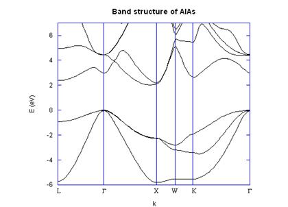
Fig. 3
In conclusion, the empirical pseudopotential method was used to calculate three band
diagrams, including AlAs, for which the form factors
were not previously known.
6. References
1. J.C. Phillips, “Energy-Band
Interpolation Scheme Based on a Pseudopotential,”
Phys. Rev. 112, 685 (1958).
2. J.C. Phillips and L. Kleinman, “New Method for Calculating Wave Functions in
3. L. Kleinman
and J.C. Phillips, “Crystal Potential and Energy Bands of Semiconductors. III.
Self-Consistent Calculations for Silicon,” Phys. Rev. 118, 1153 (1960).
4. A.A. Maradudin,
and A.R. McGurn, “Out of plane propagation of
electromagnetic waves in a two-dimensional periodic dielectric medium,” J. of
Mod. Optics, 41, 275 (1994).
5. Marvin L. Cohen and T.K. Bergstresser, “Band Structures and Pseudopotential
Form Factors for Fourteen Semiconductors of the Diamond and Zinc-blende Structures,”
Phys. Rev. 141, 2, p. 789 (1966).
6. Umberto Ravaioli
and Singh T. Junior, “The Empirical Pseudopotential
Method,” http://www-ncce.ceg.uiuc.edu/tutorials/bandstructure/pseudo.html,
downloaded November, 1995 (link now inactive).
7. DAMOCLES: Numerical algorithms – Band structure and
scattering rates. http://www.research.ibm.com/DAMOCLES/html_files/numerics.html,
downloaded November 6, 2002.
8. I. Vurgaftman,
J.R. Meyer, and L.R. Ram-Mohan, “Band parameters for III-V compounds and their
alloys,” J. of Appl. Phys. 89, 11 (2001).
9. James R. Chelikowsky
and Marvin L. Cohen, “Nonlocal pseudopotential
calculations for the electronic structure of eleven diamond and zincblende semiconductors,” Phys. Rev. B 14, 2
(1976).
10. D.J. Stukel
and R.N. Euwema, “Energy-Band Structure of Aluminum
Arsenide,” Phys. Rev. 188, 3 (1969).
7. Acknowledgements
Thanks to Emmanuel Van Kerschaver, for
pointing out a mistake in the orthogonal function (Jan. 10, 2008), and to Tim
Saucer at the